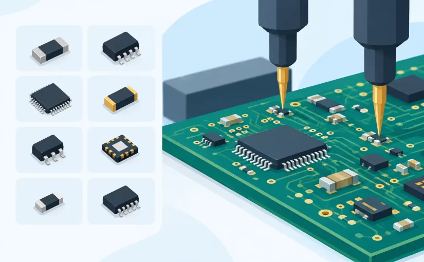
A 0402 capacitor and a SOT-23 transistor can occupy only a few square millimeters, yet each can stop a board from operating correctly. A useful surface mount package guide is therefore more than a naming reference. It connects the package on the PCB to its pad geometry, thermal behavior, assembly risks, and the practical limits of in-circuit measurement.
For repair, inspection, and production work, package identification is the first decision point. It tells the operator where the terminals are, what nearby conductors may affect a reading, whether heat can safely be applied, and which probe or tweezer tip can make repeatable contact.
Why the Package Matters Before You Measure
A surface-mount device package defines the component’s physical interface to the board. The electrical function may be familiar – resistor, capacitor, diode, MOSFET, regulator, or integrated circuit – but the package determines how that function is accessed. A 0603 resistor has exposed end terminations that are easy to contact with fine test tweezers. A QFN has contacts beneath its body, making direct pin access more limited. A BGA hides nearly all solder joints under the package and changes the inspection process completely.
Package size also affects parasitics. At low frequencies, a nominal 10 nF capacitor may look similar whether it is housed in 0805 or 0201. At higher test frequencies, lead structure, termination geometry, dielectric construction, and mounting layout have a greater influence. The measured result may include the component, its solder joints, and parallel or series paths on the PCB.
This is why a component value alone is not enough for diagnosis. Identify the package, study its connections, then select a measurement method that matches the device and circuit conditions.
Common Surface-Mount Package Families
Chip resistors, capacitors, and inductors
Rectangular chip components are commonly designated by codes such as 1206, 0805, 0603, 0402, and 0201. In the imperial system, an 0603 package measures approximately 0.06 by 0.03 inches. Metric package designations are also used, so confirm the convention in a bill of materials or manufacturer drawing before ordering replacements.
These packages usually have two metallized end terminations. Their simple construction makes them suitable for direct two-terminal measurement, but circuit context still matters. A resistor can often be checked in circuit when no alternate current path is present. Capacitors and inductors are more likely to be affected by surrounding components, power planes, and semiconductor junctions.
Larger chip packages dissipate more heat and are generally easier to rework. Smaller packages reduce board area and can improve high-frequency layout, but their solder fillets are harder to inspect and their terminations demand accurate probe placement.
Diodes, transistors, and small-outline power devices
SOT-23, SOT-23-5, SOT-89, SOD-123, SOD-323, and SMA/SMB-style packages are common in switching, protection, and regulation circuits. Their terminal arrangement must be verified from the specific part documentation. Two devices in the same SOT-23 outline can have different pin assignments and entirely different functions.
For a diode or transistor, begin with the package orientation mark and locate pin 1 or the cathode marking. Then use diode-test or controlled LCR measurement as appropriate. In-circuit diode readings can be misleading when parallel diodes, IC inputs, or charged capacitors are present. Compare with a known-good channel or isolate one terminal when the circuit does not support a clear diagnosis.
SOIC, TSSOP, QFP, QFN, and DFN packages
Leaded IC packages such as SOIC, TSSOP, and QFP expose their gull-wing leads at the package perimeter. They can be visually inspected for bridges, lifted leads, insufficient solder, and corrosion. Fine-pitch spacing increases the chance that a conventional probe tip will contact adjacent pins, so probe geometry becomes a safety and accuracy issue.
QFN and DFN packages have pads underneath or partly underneath the body. They reduce inductance and package height, but center thermal pads and hidden side contacts complicate inspection. A failed QFN is often diagnosed through accessible decoupling capacitors, nearby resistors, exposed test points, or signal behavior rather than direct contact with every package terminal.
BGA and chip-scale packages
Ball grid arrays place solder balls beneath the package. They provide high I/O density and favorable electrical performance, especially for processors, memory, and high-speed devices. Their trade-off is accessibility: optical inspection cannot confirm every solder joint, and rework requires controlled heating, alignment, and usually X-ray or other specialized inspection methods.
At board level, BGA troubleshooting often starts with rail resistance, decoupling-capacitor measurements, clock and reset checks, and thermal observations. Package identification still guides the work, but the useful test points are often outside the device footprint.
Reading Markings, Orientation, and Footprints
Package markings are helpful but not always unique. A two- or three-character top mark may identify multiple devices from different manufacturers. Use it alongside package dimensions, pin count, board reference designator, circuit position, and surrounding components. The marking alone is rarely adequate evidence for replacement selection.
Orientation indicators deserve the same care. Dots, chamfered corners, molded dimples, laser marks, bars, and cathode bands may indicate pin 1 or polarity. On a board, the silkscreen may be incomplete, obscured by the part, or inconsistent with a revision change. Verify orientation from copper pads and the schematic when available.
The footprint is the PCB land pattern intended for the package. It establishes pad width, spacing, solder-mask clearance, paste aperture, and thermal connection. A part can be the correct nominal package yet be unsuitable if its terminal style or recommended land pattern differs. This occurs frequently with QFN thermal pads, diode packages, and chip capacitors from different vendors.
A Surface Mount Package Guide for Measurement Work
Measurement begins with safe board conditions. Remove power, discharge capacitors where necessary, and consider whether the circuit may contain battery-backed rails or charged high-voltage sections. Then inspect the component under magnification before placing probes. Cracked bodies, tombstoned chip components, solder voids, discolored terminations, and pad lifting can explain a failure before any numerical reading is taken.
For two-terminal components, clean contacts and correct tip pressure are central to repeatability. Excess pressure can slide an 0201 part, fracture a ceramic capacitor, or create intermittent contact. Too little pressure can add unstable resistance. Fine, gold-plated tweezer probes provide a controlled way to contact both terminations without shorting adjacent pads.
Test frequency should match the question being asked. A low-frequency capacitance measurement may confirm that a capacitor is not open or grossly shorted. Higher-frequency LCR and ESR measurements can better reveal behavior relevant to switching supplies, RF bypassing, and low-impedance ceramic capacitors. Results should be compared against the expected tolerance, package type, dielectric, and circuit topology – not merely the nominal printed value.
In-circuit readings require judgment. A resistor across an IC input may measure lower than its marked value because other paths are in parallel. A capacitor on a power rail may show a low apparent impedance because dozens of capacitors share the rail. If the reading is questionable, lift one end only when the board, component value, and repair economics justify it.
Compact instruments designed for SMD work reduce handling time because the operator can grip a loose component or contact installed end caps directly. Siborg Smart Tweezers and LCR-Reader instruments are intended for this workflow, with automatic component identification on supported models and measurement options suited to component-level PCB diagnosis. For controlled documentation, calibration status and measurement conditions should be recorded with the result.
Selecting a Replacement Package
A replacement must match more than capacitance, resistance, or semiconductor part number. Confirm the package outline, terminal count, polarity, voltage rating, power dissipation, current capability, tolerance, temperature coefficient, dielectric class, and thermal requirements. For capacitors, a physically smaller package may lose effective capacitance under DC bias. For resistors, pulse rating and working voltage can matter more than nominal wattage.
Do not substitute a larger package simply because it fits across the pads, or a smaller one simply because it is available. Incorrect pad coverage can produce weak solder joints, poor heat transfer, tombstoning, and altered high-frequency behavior. When a board uses a tightly specified footprint, the original manufacturer package drawing is the practical reference.
Build Identification Into the Test Process
Treat package identification as a measurement parameter, alongside range, test frequency, and calibration state. Record the package code or measured body dimensions when documenting a suspect component, especially when top markings are ambiguous or a board has multiple revisions. That small habit makes later comparison, procurement, and failure analysis far more reliable.
The fastest component test is not necessarily the one that produces the first number. It is the one that identifies the package, reaches the correct terminals, accounts for the surrounding circuit, and produces a result you can trust.