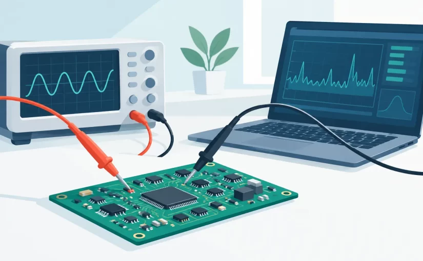
Digital Component Tester for PCB Diagnostics

A failed board rarely presents one obvious bad part. A power rail may collapse because of a shorted ceramic capacitor, an intermittent inductor, a resistor installed with the wrong value, or a semiconductor fault elsewhere on the net. A digital component tester shortens that search by bringing direct identification and measurement to the component itself, especially where conventional probes are too large or too slow for densely populated PCB assemblies.

For engineers, repair technicians, and quality teams, the useful question is not whether an instrument can produce a reading. It is whether that reading is made at a suitable test frequency, with adequate accuracy, repeatable contact, and enough context to support a repair or production decision.

What a Digital Component Tester Should Measure

A basic component tester can identify common passive components and provide approximate values. That can be useful on loose through-hole parts, incoming inspection, or sorting mixed inventory. PCB diagnostics usually demand more. Small SMD components, parallel paths, solder flux residue, and nearby semiconductors can all affect an in-circuit measurement.

A professional digital component tester should measure resistance, capacitance, and inductance with clearly defined test conditions. ESR measurement is particularly useful when evaluating electrolytic capacitors, polymer capacitors, and other parts whose capacitance may appear acceptable while their loss characteristics have changed. Diode and transistor functions can help with initial semiconductor checks, although they do not replace application-specific circuit analysis.

Test frequency matters because component behavior changes with frequency. An inductor measured at a low frequency can appear satisfactory but behave differently in a switching circuit. Capacitors also have frequency-dependent impedance and dissipation characteristics. Instruments offering 100 kHz or 250 kHz test capability provide a more relevant view for many high-frequency, switching-power, RF-adjacent, and compact digital designs than low-frequency-only measurements.

Accuracy should be evaluated beyond the headline specification. Basic accuracy of 0.1% or 0.2% is valuable, but real measurement confidence also depends on probe condition, contact resistance, calibration status, component range, and the selected measurement mode. An instrument should state its accuracy, test signal, frequency, and measurement range clearly enough for the user to judge whether it fits the task.

Why Tweezer-Style Probing Changes PCB Work

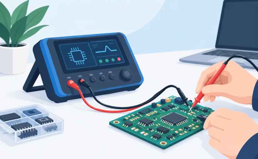
The limiting factor in component testing is often not the measurement engine. It is physical access. Standard multimeter leads can bridge adjacent pads, slip off 0402 or 0201 packages, or require a third hand to hold the board and probes in place. Fine test tweezers place both measurement contacts at the component terminals in one motion.

This approach improves speed, but its greater value is consistency. The same controlled contact pressure and short probe path can reduce the variable introduced by loose leads and improvised clips. On crowded boards, a technician can isolate a chip resistor, capacitor, or inductor without placing two large probe tips across neighboring circuitry.

For loose SMD parts, tweezers also reduce handling time. A technician can pick up a component, measure it, and place it in a labeled tray without changing tools. For production inspection and rework verification, that repeated workflow is more efficient than using separate probes for every part.

Siborg Systems’ Smart Tweezers instruments are designed around this direct-contact method, combining tweezer-style probing with LCR measurement for loose and in-circuit component work. The configuration is especially practical when the board layout, rather than the component specification, is the primary obstacle.

In-Circuit Readings Require Judgment

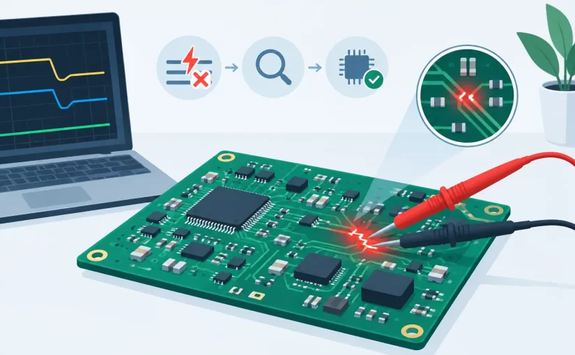
No digital component tester can fully separate a component from every circuit path while it remains soldered to a board. A resistor may be shunted by another resistor or an IC input. A capacitor may be effectively paralleled by several capacitors on the same supply rail. An inductor may share a path through a switching controller, diode, or transformer winding.

The correct approach is to treat an in-circuit result as diagnostic evidence, not automatic proof. If a 10-ohm resistor reads 2 ohms in circuit, the reading may indicate a failed resistor, but it may also show a legitimate parallel load. Compare with a known-good board where possible. Check the schematic, boardview data, or neighboring channels. If the result remains questionable, lift one terminal and remeasure the part out of circuit.

Capacitor troubleshooting illustrates this distinction well. A low-resistance rail-to-ground reading can identify a shorted area quickly, but a component tester alone may not identify which capacitor is defective when many are in parallel. The tester is strongest when used with a structured workflow: locate the abnormal net, identify candidate components, compare measurements, and confirm by isolation when needed.

Selecting the Right Measurement Capabilities

Instrument selection should begin with the boards and components being serviced. A technician repairing consumer power supplies has different priorities from an engineer validating RF matching networks or a manufacturer checking SMD reels.

For general PCB repair, resistance, capacitance, inductance, diode testing, and ESR provide a solid starting point. For switching supplies and modern compact electronics, higher test frequency and reliable low-value measurement become more significant. Low inductance, low resistance, and small ceramic capacitors are common precisely where poor probes and limited frequency capability can produce misleading results.

Consider these operational requirements before selecting a tester:

  • Basic accuracy and resolution: Determine whether the instrument can distinguish the tolerances and fault levels relevant to the components under test.
  • Available test frequencies: Higher-frequency LCR testing can better represent components used in switching and high-speed circuits.
  • In-circuit usability: Fine probes or tweezers should reach small packages without contacting adjacent pads.
  • Calibration documentation: NIST-traceable calibration certificates support quality systems, formal labs, and measurement records.
  • Data capture: Bluetooth or PC-connected capability is useful when readings must be logged, reviewed, or transferred to a report.
  • Advanced diagnostic functions: Oscilloscope and Analog Signature Analysis modes can add fault-isolation options beyond passive component measurement.

Not every user needs every function. A bench technician sorting components may place the highest value on speed and automatic identification. A field service specialist may prioritize portability, battery operation, and repeatable in-circuit access. An engineering lab may need traceable calibration, high-frequency testing, and digital records. Buying for the actual workflow is more useful than comparing a single specification in isolation.

A Practical PCB Diagnostic Sequence

Begin with visual inspection. Look for cracked MLCCs, discolored resistors, lifted pads, corrosion, damaged connectors, and heat-stressed electrolytics. A tester cannot compensate for a missed physical defect.

Next, power down the board and discharge capacitors as required. Measuring a charged capacitor or energized circuit risks damaging both the instrument and the board. Check suspect power rails for an abnormal resistance-to-ground condition, then use the component tester to compare nearby components and identify values that differ from equivalent locations.

When measuring a passive component, let the instrument settle before recording the result. Clean oxidized terminals when practical, and verify that tweezer tips are properly aligned and free of contamination. If the reading changes noticeably with probe pressure or position, contact quality may be the problem rather than the part.

For board-level faults that remain ambiguous, add other methods rather than forcing a conclusion from one measurement. A thermal camera, controlled current injection, oscilloscope trace, or Analog Signature Analysis comparison can reveal behavior that static LCR testing cannot. Effective troubleshooting is a sequence of increasingly specific evidence, not a single test.

Protecting Measurement Confidence Over Time

A precision instrument remains useful only when its probes, calibration, and handling are maintained. Fine tweezer tips are wear items. Bent, contaminated, or heavily oxidized tips can raise contact resistance and create unstable readings, particularly on low-ohm components and small pads. Replace or service accessories before they become a source of uncertainty.

Calibration is equally practical, not merely administrative. For organizations documenting repair quality or validating production measurements, a current NIST-traceable calibration certificate provides a defensible reference point. Even for independent technicians, periodic verification against known standards helps identify drift or damaged probes before a questionable measurement reaches a customer report.

A digital component tester earns its place on the bench when it reduces uncertainty at the exact point where troubleshooting slows down: the individual part on a crowded PCB. Select measurement frequency, accuracy, probing method, and documentation capabilities for the boards you actually service, then use the instrument as part of a disciplined diagnostic process. The result is not just a faster reading, but a better-supported decision about what to repair, replace, or investigate next.
Best Tools for SMD Rework at Your Bench

A 0402 capacitor can be removed in seconds and still leave a repair that fails under load. The difference is rarely just operator skill. The best tools for SMD rework give the technician control over heat, access, alignment, and verification before the board returns to service.

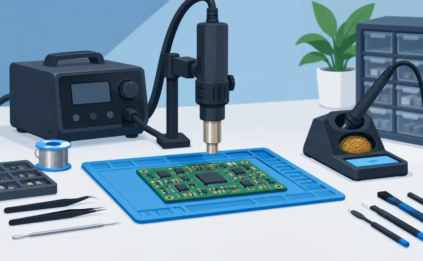
SMD rework is a system, not a single tool purchase. Hot air without stable board support can lift pads. A fine soldering iron without proper magnification can bridge adjacent pins. A replacement component selected only by its marking can introduce a fault that looks identical to the original failure. Build the bench around the component sizes, board density, and volume of work you actually handle.

Best Tools for SMD Rework: Start With Heat Control

A temperature-controlled soldering iron is the primary tool for resistors, capacitors, jumpers, small diode packages, and touch-up work. Select a station with fast thermal recovery and cartridges or tips suited to the work, rather than relying on one ultra-fine conical tip for everything. A small chisel or hoof tip transfers heat more efficiently to most pads and allows controlled drag soldering on fine-pitch leads.

For production-quality work, temperature stability matters more than a high maximum temperature rating. Excessive tip temperature oxidizes flux quickly, damages pads, and increases the chance of heat traveling into adjacent components. Start with a temperature appropriate for the alloy, tip geometry, ground-plane connection, and thermal mass of the joint. Adjust based on observed wetting performance, not habit.

A hot-air rework station is necessary for QFNs, SOICs, chip components, shielded areas, and parts with contacts underneath the package. Look for adjustable airflow as well as temperature control. High airflow can displace 0201 and 0402 parts long before the solder reaches reflow temperature. Low, directed airflow combined with a nozzle sized close to the package gives better local control.

Preheating becomes valuable when working on multilayer boards, large ground planes, heavy connectors, or lead-free assemblies. A board preheater reduces the thermal gradient between the top-side rework area and the rest of the PCB. This shortens hot-air exposure and reduces the risk of pad lifting, board warpage, and repeated heating of nearby components. It is not mandatory for every repair, but it pays for itself quickly on dense or thermally demanding boards.

Magnification and Lighting Prevent Expensive Rework

Inspection should happen before removal, after pad preparation, and after soldering. A stereo microscope remains the most practical option for manual rework because it provides depth perception. That makes it easier to position a QFN, inspect solder fillets, identify lifted lands, and judge whether a component is sitting flat.

A digital microscope is useful for documentation, training, and sharing images with a customer or engineering team. It may be less comfortable for continuous hand work if display latency or limited depth perception gets in the way. Many repair benches use both: a stereo microscope for placement and soldering, then a digital camera or microscope for records.

Use bright, adjustable illumination with minimal shadowing. Ring lights are common, but angled side lighting can reveal tombstoning, solder bridges, cracked terminations, and damaged traces that direct overhead light can hide. The goal is not maximum brightness. It is clear contrast at the working distance you use.

Board Holding and Hand Tools Matter More Than They Look

A stable PCB holder is one of the most effective upgrades for repeatable SMD work. It should secure the board without flexing it, allow access from multiple sides, and tolerate localized heat. Magnetic holders can be convenient, while adjustable edge clamps are better for irregularly shaped boards. Avoid clamping directly on delicate connectors, test points, or flex sections.

Precision tweezers are required for placement and removal, but tip selection should match the package. Very sharp tips are useful for fine-pitch work, while broader curved tips offer more secure control of 0603 and larger chip parts. ESD-safe construction is appropriate when handling sensitive semiconductors, and clean tips reduce the risk of contaminating pads with residue.

Keep a nonmagnetic spudger, fine picks, a scalpel or trace-cutting knife, and small flush cutters available for repair tasks. These are not substitutes for proper heating. They are support tools for removing adhesive, separating a component after solder has reflowed, repairing solder mask edges, or preparing a damaged trace.

When a board must be held at an angle, use a fixture that does not force your hands into an awkward position. Poor ergonomics shows up as shaky placement, inconsistent iron contact time, and damaged pads during long repair sessions.

Flux, Solder, and Consumables Set the Process Window

No-clean flux is a practical default for many board repairs, but flux type should be chosen for the assembly and cleaning requirements. Tacky flux keeps small parts from moving during hot-air work. Liquid flux is useful for drag soldering and for improving heat transfer during component removal. Water-soluble flux can be highly active, but residues must be cleaned thoroughly.

Use solder wire sized for the work. Fine wire gives better volume control on small pads; larger wire is more efficient for connectors and heavier joints. For lead-free boards, adding a small amount of compatible alloy or low-melting-point removal alloy can lower the effort needed to remove a part, but it must be fully removed from the pads before installing the replacement component.

Solder wick is essential for pad cleanup and bridge removal. Choose a width that matches the land pattern. Oversized wick can pull heat from the joint and increase the time the board is exposed to the iron. Used correctly with flux, it leaves flat, solderable pads without scraping or excessive abrasion.

Kapton tape and heat shields protect neighboring components during hot-air work. They help, but they are not a guarantee. Sensitive plastic connectors, microphones, switches, and electrolytic capacitors may still require local shielding, reduced airflow, or removal before rework begins.

Verify Components Before and After Installation

A successful solder joint does not prove the installed part is correct. This is where a dedicated LCR meter or SMD test tweezers become more useful than conventional test leads. Direct tweezer measurement lets the technician identify loose resistors, capacitors, inductors, and semiconductors quickly, with less risk of slipping across adjacent pads.

In-circuit readings require judgment. Parallel paths, semiconductor junctions, and surrounding capacitance can influence the value. Compare with a known-good channel or an equivalent location on the board when possible. If the result is ambiguous, lift one end of the component or test the replacement part before installation.

For high-frequency or low-impedance components, test frequency and basic accuracy affect whether a reading is meaningful. Instruments such as Siborg Smart Tweezers and LCR-Reader models are designed for direct SMD contact, with configurations offering up to 250 kHz test frequency, accuracy options down to 0.1%, and features such as ESR measurement. Those capabilities are especially relevant when verifying small capacitors, inductors, and low-value resistors where a basic multimeter cannot provide enough information.

A digital multimeter remains necessary for continuity checks, voltage rails, diode tests, and gross resistance faults. It complements, rather than replaces, a purpose-built LCR instrument. For difficult intermittent faults, oscilloscope capability and Analog Signature Analysis can add another layer of evidence before parts are removed unnecessarily.

Choose the Tool Set for the Job, Not the Catalog

A technician repairing consumer boards occasionally can begin with a controlled iron, compact hot-air station, quality flux, tweezers, microscope, board holder, and reliable measurement instrument. A service department handling multilayer industrial boards should add preheating, dedicated nozzles, documented calibration, ESD controls, and a workflow for recording measurements.

For fine-pitch IC replacement, component alignment and thermal control deserve more budget than specialty hand tools. For passive-component troubleshooting, fast and accurate direct measurement often has the largest effect on turnaround time. For high-volume rework, fixtures and repeatable thermal profiles become the priority.

The practical standard is simple: use enough heat to form or reflow the joint quickly, enough magnification to inspect it honestly, and enough measurement capability to prove the component and repair are correct. That approach produces fewer repeat repairs and gives every board a better chance of leaving the bench fixed for the right reason.

How to Check PCB Continuity Without False Reads

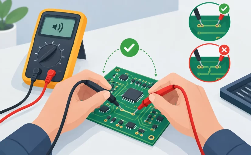
A continuity beep is useful only when it answers a specific question. On a populated board, adjacent nets may be connected through low-resistance components, IC protection structures, relay contacts, or parallel circuitry. Knowing how to check PCB continuity means proving the intended conductive path while recognizing when an audible indication is not sufficient evidence.

For PCB repair, production inspection, and field service, continuity testing is primarily used to find open traces, cracked vias, poor solder joints, damaged connector paths, and unintended shorts. The meter is simple. The interpretation requires a method.

What PCB Continuity Testing Actually Verifies

Continuity mode applies a small test signal between two probes and indicates that the resistance is below the instrument’s continuity threshold. Depending on the meter, that threshold may be anywhere from a few ohms to several tens of ohms. A beep therefore means low resistance, not necessarily a direct copper short.

This distinction matters on dense assemblies. A 0-ohm jumper, inductor, fuse, relay contact, low-value current-sense resistor, or power distribution network can all produce a valid continuity indication. Conversely, a corroded trace or marginal solder joint may measure several ohms and fail to trigger the buzzer even though some electrical connection remains.

Use continuity mode for fast go/no-go checks. When the result affects a repair decision, switch to resistance mode and record the reading. A stable resistance value provides more diagnostic information than a beep alone.

Set Up the Board and Meter Correctly

De-energize the PCB before connecting a continuity tester. Disconnect the main supply, battery, USB connection, external programmer, and any source that can backfeed the board. Continuity mode is not intended for measurements on live circuits, and external voltage can damage the meter or produce misleading results.

Large capacitors deserve special attention. After power is removed, verify that bulk capacitors and high-voltage sections have discharged. Use the correct discharge procedure for the equipment and its stored energy. Do not intentionally short a charged capacitor with a probe tip.

Inspect the test leads before blaming the PCB. Touch the probe tips together and observe both the audible response and displayed resistance. A professional DMM should show a low, repeatable value, but the exact result includes lead and contact resistance. Flex the leads near the strain reliefs while testing. Intermittent leads can imitate an intermittent board fault.

For fine-pitch work, standard pointed probes are often too large. Sharp micro-probes, pogo probes, or tweezer-style contacts reduce the chance of bridging neighboring pads. The goal is controlled contact on the intended copper feature, not simply obtaining a beep.

How to Check PCB Continuity Step by Step

Start with the schematic, board layout, assembly drawing, or a known-good board whenever possible. Define the net you expect to follow. For example, you may need to verify a signal from a connector pin to a series resistor, from that resistor to an IC pin, and from the IC pin through a via to another layer.

Place one probe on a known point on the net, such as a connector terminal, test point, component pad, or exposed via. Place the second probe at the expected destination. Hold both probes steadily and wait for the reading to settle. Oxidized pads, conformal coating, flux residue, and probe movement can cause momentary or unstable results.

If continuity is present, move the second probe along the signal path. Check both sides of series components, each accessible via, and each connector transition. This divides the net into smaller sections and localizes the fault quickly. A good connection up to one via and an open reading after it identifies the region that needs magnification and inspection.

If continuity is absent, do not immediately scrape solder mask or replace a component. First confirm that the two points are intended to be on the same net. Then inspect for a series resistor, ferrite bead, fuse, switch, transistor junction, or connector contact between them. The open reading may be correct by design.

When testing a suspected short, place probes on the two nets that should be isolated. A low reading may indicate a solder bridge, conductive contamination, damaged IC, failed capacitor, or an alternate path elsewhere in the circuit. Compare the resistance with an equivalent channel or a known-good assembly if available.

Test the Most Common Failure Points

Traces and vias

A trace can look intact while being open beneath a component, inside a flex region, or under corrosion. Test from one end of the trace to the other, then test at intermediate points. For multilayer boards, test each via from its top-side land to the corresponding bottom-side land where accessible.

A via may be mechanically present but electrically unreliable because of barrel cracking or poor plating. Flexing the board is not a preferred test method because it can worsen the damage. Instead, monitor resistance while applying only minimal, controlled pressure near the suspect area.

Solder joints and SMD pads

Continuity between a component lead and its pad confirms little if the pad itself has lifted from the trace. Test from the component terminal to a downstream via or another point on the same net. On small surface-mount devices, direct tweezer contacts can be faster and more repeatable than trying to balance two conventional probes on adjacent terminations.

For components with multiple parallel connections, isolate the question. Test a resistor pad to its trace, then test across the resistor separately. This prevents the component value from being confused with the integrity of the copper path.

Connectors, cables, switches, and fuses

Connector faults often occur at the solder tail, crimp, plated contact, or cable strain point. Test pin-to-pin while gently moving the cable or operating the mating mechanism. A reading that changes with movement is evidence of an intermittent mechanical connection.

For switches and relays, compare the measured state with the specified contact state. Closed contacts should have low and stable resistance. If the meter beeps but the resistance is higher than expected for the application, measure it quantitatively. A few ohms may be unacceptable in a power path even though continuity mode reports a connection.

A fuse should normally show near-zero resistance in circuit. If a low value is questionable because of parallel circuitry, lift one end or use the board documentation to identify alternate paths.

Avoid False Positives on Populated Boards

Semiconductor junctions are a common source of confusion. Depending on probe polarity and meter test voltage, an ESD diode or transistor junction can conduct in one direction and appear open in the other. Reverse the probes and compare the behavior. Use diode-test mode when the question is junction behavior rather than copper continuity.

Capacitors can briefly conduct as they charge from the meter’s test source. The display may start low and rise, or the buzzer may chirp momentarily. Wait for the reading to stabilize. A persistent low resistance across a power rail is more suspicious than a transient indication, but even that requires comparison against the design and nearby circuit sections.

Parallel paths are unavoidable in many circuits. A signal may return through an IC, a pull-up network, a transformer winding, or another channel. If the board architecture is complex, isolate the path by removing a connector, opening a jumper, lifting one component terminal, or testing an unpopulated equivalent board. Isolation is slower, but it turns an ambiguous result into a defensible measurement.

Select the Right Instrument and Probe Method

A digital multimeter is the primary tool for continuity work, provided its beeper response is fast enough and its resistance range is appropriate for low-ohm verification. For boards with very small components, probe geometry can have more effect on speed than the meter itself.

SMD test tweezers are particularly effective for measuring directly across chip resistors, fuses, inductors, and capacitors without chasing small pads with separate leads. An LCR meter or ESR meter does not replace continuity mode, but it adds component-level evidence when a part appears electrically connected yet behaves incorrectly in circuit. For example, a shorted multilayer ceramic capacitor and a normal low-resistance power rail require different follow-up tests.

Siborg’s handheld tweezer-style instruments are designed for direct contact with small SMD terminations, helping technicians separate a trace fault from a component fault without unnecessary board handling. For documented service work, use calibrated instruments and record readings when acceptance criteria require traceability.

When Continuity Is Not Enough

Continuity testing cannot confirm current-carrying capability, insulation performance at operating voltage, high-frequency signal integrity, or the health of a component under load. A cracked trace may pass a low-current meter test and fail when the circuit draws current. A connector contact may read low resistance at rest but develop voltage drop under vibration or load.

Follow a successful continuity check with the test that matches the failure mode. Measure voltage drop for power paths, use four-wire resistance measurement for very low-resistance connections, perform insulation testing where safety requirements apply, or examine high-speed signals with an oscilloscope. Continuity narrows the fault location. It does not replace functional verification.

The most efficient PCB troubleshooting habit is to treat every beep as a data point, not a verdict. Test the intended net, compare the resistance to the circuit expectation, and isolate uncertain paths before rework. That approach protects pads, reduces repeat repairs, and produces measurements that can be trusted.

How to Capture Measurement Data from PCBs

A board repair record that says “capacitor tested bad” is rarely useful six weeks later. A record that identifies the board revision, reference designator, test frequency, measured capacitance, ESR, bias condition, and instrument status can be checked, repeated, and defended. That distinction is central to how to capture measurement data when troubleshooting populated PCBs, qualifying incoming components, or documenting production results.

The objective is not to collect the largest possible number of readings. It is to capture readings that retain their measurement context. A value without test conditions may look precise while being impossible to compare with a later result.

Start with a defined measurement objective

Before placing probes on a component, determine what decision the measurement must support. A technician locating a shorted ceramic capacitor needs a fast comparison between rails or like circuits. A quality-control operator verifying an inductor lot needs controlled test frequency, fixture consistency, and acceptance limits. An engineer characterizing a circuit may need a time-based waveform in addition to L, C, R, or ESR values.

This objective determines the required instrument, range, test frequency, and record format. Resistance measured with a DMM is not interchangeable with impedance measured by an LCR meter. Likewise, a capacitance reading at 1 kHz may not predict behavior at 100 kHz or 250 kHz. For components used in switching supplies, RF-adjacent circuits, and high-speed bypass networks, frequency selection can materially change the useful result.

Record the expected value or acceptable range before testing when possible. This prevents a common troubleshooting error: treating the first displayed number as proof that a component is good.

Control the conditions before capturing data

Good data begins with a stable setup. Verify that the PCB is unpowered and discharged unless the procedure specifically requires powered-circuit measurements. Stored energy in capacitors can damage an instrument, distort readings, and create a safety hazard.

For loose components, use clean contacts and a repeatable fixture or probe position. For populated boards, identify all parallel paths before interpreting an in-circuit result. A resistor can appear lower in value because another circuit path is in parallel. A capacitor can appear larger or have a lower apparent ESR because other capacitors share the same rail. Semiconductors, IC protection structures, and leakage paths can also influence the result.

This does not make in-circuit measurement ineffective. It changes what the reading means. In-circuit readings are often highly effective for comparative diagnosis: compare an identical channel, a known-good board, or neighboring components of the same design. When the result is close to a decision limit, isolate one lead or remove the component for confirmation.

Environmental conditions also matter for close-tolerance work. Temperature affects resistance, capacitance, and semiconductor behavior. Allow the board and instrument to stabilize after moving from a cold service vehicle into a warm lab. Keep fingers away from exposed component terminals during high-resistance measurements, where body leakage can become part of the reading.

Select the measurement method that matches the component

The fastest measurement is not always the right measurement. Choose the mode and connection method based on the component and failure mode under investigation.

For resistors, confirm whether a simple DC resistance reading is sufficient or whether in-circuit paths require comparison or isolation. For capacitors, capture capacitance and ESR when both values affect the diagnosis. A capacitor may remain near nominal capacitance while its ESR has increased enough to cause ripple, startup, or regulation problems.

For inductors, record inductance at a relevant test frequency and note DC resistance if winding loss or open connections are concerns. For diodes and LEDs, capture forward voltage at a stated test current where the instrument supports it. A visual pass/fail result alone is not adequate for documenting marginal devices.

Tweezer-style LCR instruments are particularly useful for small SMD parts because they reduce lead length, contact uncertainty, and time spent positioning conventional probes. On densely populated boards, insulated probe arms and fine tips can help reach a component without bridging adjacent pads. The contact method should still be documented when measurements are close to specification, since oxidation, probe pressure, and contact point can alter low-value resistance and ESR results.

How to capture measurement data with useful context

A useful record combines the measured value with the information needed to reproduce it. At minimum, each entry should identify the board or assembly, location, component type, value, units, and test conditions. For professional troubleshooting and quality records, capture these fields consistently:

  • Board model, serial number, revision, and work order or case number
  • Reference designator and a brief component description
  • Measurement function, test frequency, range, and equivalent circuit setting when applicable
  • Measured result, units, tolerance limit, and pass, fail, or comparison status
  • Instrument model, asset number, calibration status, date, and operator

The equivalent circuit setting deserves attention. LCR meters may present series or parallel values, such as Cs-Rs or Cp-Rp. Neither is universally correct. A low-impedance capacitor at higher frequency is often better represented by a series model, while a high-impedance component may be better represented by a parallel model. The key is to select the appropriate model for the application and use it consistently across comparable readings.

Do not round away diagnostic information too early. If the instrument reports 0.184 ohms ESR, recording “0.2 ohms” may be adequate for a broad service note but not for a trend record. Save the native resolution where the measurement uncertainty supports it, then apply the acceptance limit separately.

Use digital transfer to reduce transcription errors

Manual recording remains practical for a handful of readings, but it becomes a source of errors when testing boards in quantity. Transposed decimal points, missing units, and undocumented settings can make a spreadsheet less reliable than the meter display it was copied from.

Bluetooth-enabled measurement tools provide a more controlled path for repeated work. On compatible instruments, captured readings can be transferred to a mobile device or PC while retaining timestamps and reducing manual entry. Siborg Systems instruments such as Bluetooth-enabled Smart Tweezers and LCR-Reader models are designed for component-level measurement workflows where direct access and digital transfer both matter.

Digital capture is most valuable when the receiving format is standardized. Use fixed fields for board ID, reference designator, measurement type, limits, and technician notes. If a measurement is tied to a photo, thermal image, or oscilloscope capture, use the same work-order identifier across every file. That creates a record that can be reviewed without guessing which board or test point the data belongs to.

For small repair operations, a structured CSV file may be sufficient. For production or calibration-controlled environments, integrate readings into the existing quality system and preserve revision history. The best method depends on volume, traceability requirements, and whether the data will be used for trend analysis rather than a single repair decision.

Verify the instrument and the data

A precise display does not guarantee a valid measurement. Inspect probe tips, leads, and tweezer arms for contamination, wear, looseness, or damaged insulation. Perform open and short compensation when the instrument and procedure require it, especially when measuring low impedance or using extension fixtures. Compensation removes a portion of fixture and lead effects, but it cannot correct poor component contact or a wrong test method.

Maintain calibration records appropriate to the work. A NIST-traceable calibration certificate supports documented quality processes and establishes confidence in the instrument’s performance at the time of calibration. It does not eliminate the need for a quick functional check before critical work. A known reference component or verification standard can reveal damage or setup problems between scheduled calibrations.

Review outliers before acting on them. Repeat the measurement after repositioning the probes, then compare with a known-good location or board. If the reading changes significantly, investigate contact quality, parallel circuitry, temperature, and test settings before declaring the component defective.

Turn measurements into repeatable decisions

Capture a baseline from known-good boards whenever a product family is serviced repeatedly. Baseline records are more useful than generic nominal values because they include the realities of the assembled design: tolerance stack-up, parallel networks, and normal production variation.

Over time, this turns measurement capture from documentation into a diagnostic tool. A recurring ESR shift on a certain rail, a gradual change in coil resistance, or a pattern of low LED forward voltage can reveal failure modes before they are obvious from a single board.

The next time a component reading drives a repair or release decision, capture the conditions that produced it along with the number. A measurement record should let another technician recreate the test, understand the result, and move directly to the next justified action.

PCB Fault Isolation Case Study for Shorted Rails

A board that draws 1.8 A from a 3.3 V bench supply before its processor can boot presents a familiar repair problem: the power rail is shorted, but the board contains dozens of parallel bypass capacitors and IC pins. This PCB fault isolation case study follows the measurement sequence used to identify the failed component without removing every capacitor on the rail.

The board was a compact communications module returned from field service. Its 3.3 V input rail fed a processor, memory, RF section, switching-regulator control circuitry, and more than 40 multilayer ceramic capacitors (MLCCs). A visual inspection found no cracked packages, solder bridges, discoloration, or obvious liquid contamination. The fault had to be located electrically.

The Symptom Was a Low-Resistance Power Rail

With the board disconnected from all external equipment, a digital multimeter measured 0.18 ohms from the 3.3 V rail to ground. Reversing the probes produced essentially the same reading. That value was far below the expected resistance of an inactive logic rail and explained the current-limited supply behavior.

A resistance reading alone did not identify the failed part. On a populated PCB, every capacitor, IC, protection device, and regulator input connected to the rail contributes a parallel path. A low reading can result from a shorted MLCC, failed IC, damaged transient suppressor, solder defect, or a component that is normally low impedance at the meter’s test conditions.

The first decision was therefore not which part to desolder. It was how to divide the circuit into measurable sections while preserving evidence.

PCB Fault Isolation Case Study: Establishing a Test Plan

The schematic and board layout showed that the 3.3 V source entered through a ferrite bead, then split into three major branches: the digital core area, an RF section, and an interface section. Each branch had local decoupling networks. The ferrite bead and two zero-ohm links provided convenient boundaries for isolation.

Before lifting anything, the technician recorded resistance-to-ground measurements at the source and on both sides of each isolation component. The RF branch measured 22 ohms. The interface branch measured 11 ohms. The digital core branch measured 0.21 ohms. That narrowed the search from the complete board to a 35 mm by 40 mm processor area.

This step matters because thermal methods can be misleading on a dense assembly. Injecting current into an entire rail may heat the point of lowest resistance, but that point is not always the defective part. Copper planes spread heat quickly, and a shorted capacitor beside a large BGA can be difficult to distinguish from the BGA itself. Sectional resistance measurements establish a defensible starting point.

Why In-Circuit Component Measurements Were Useful

The digital branch contained 17 MLCCs, three IC supply pin groups, and one small load switch. Removing capacitors one at a time would have been slow and would have increased the risk of pad damage. Instead, the technician compared impedance behavior at individual capacitors using tweezer-style probes.

At low test frequency, a good decoupling capacitor connected to a power plane may appear nearly identical to its neighbors because the plane and parallel capacitors dominate the reading. Higher-frequency LCR measurements provide more separation when a component has a distinct local connection or when its effective impedance differs from the surrounding network.

A handheld instrument with direct tweezer contact is particularly useful here. For example, a Siborg Smart Tweezers model with high-frequency LCR capability can contact 0402 and 0603 terminations directly, reducing probe-lead inductance and preventing accidental contact with adjacent pads. The measurement is still an in-circuit indication, not a guaranteed component value. Its value is comparative: identify the part whose behavior differs materially from similar capacitors on the same rail.

The technician measured each accessible MLCC in capacitance, resistance, and ESR modes, recording values rather than relying on a single screen reading. Most capacitors showed a stable capacitive response with low but finite ESR. One 4.7 uF, 0402 capacitor near the processor’s switching supply pins showed a resistance-dominant response and near-zero impedance across multiple test conditions. Its adjacent capacitors did not.

That result was suspicious, but not enough to condemn the capacitor. The part could have been connected very close to a shorted processor supply ball.

Controlled Current Injection Confirmed the Area

The isolated digital branch was supplied with 0.8 V and a current limit of 1.5 A. The low voltage was selected to avoid forward-biasing semiconductor junctions or powering logic unintentionally. The branch immediately reached the current limit.

After approximately 20 seconds, thermal inspection showed a small temperature rise near the suspect capacitor. The processor package also warmed slightly because it shared the same copper region, but the capacitor’s temperature increased first and more rapidly. This was a useful confirmation, not a final diagnosis.

Current injection should be applied carefully. The appropriate voltage depends on the rail, attached devices, and likely failure mode. A rail containing ESD structures, battery-management ICs, or multiple regulator paths can conduct through protection diodes at voltages that would not normally be present during operation. Start below a typical semiconductor junction threshold where practical, set a conservative current limit, and monitor the board continuously.

Removal Turned Suspicion Into Evidence

The suspect MLCC was removed with controlled hot air and the pads were cleaned. The rail resistance immediately increased from 0.21 ohms to 38 ohms. The removed component measured as a near-short out of circuit. A replacement capacitor restored normal rail behavior, and the board’s startup current returned to its expected level.

The repair was then verified beyond the original symptom. The technician checked regulator output, processor boot activity, communication function, and rail ripple under normal load. A repaired board can pass a resistance check yet still contain a marginal regulator, damaged load, or secondary defect caused by the original event.

What Made This Fault Isolation Efficient

The key was the order of operations. Visual inspection eliminated obvious assembly defects. Resistance mapping across existing branch points localized the problem. Comparative in-circuit measurements identified an outlier. Controlled current injection correlated that electrical outlier with localized heating. Only then was a component removed.

This approach is faster than indiscriminate rework, but it has limits. If the short sits under a BGA, inside an IC, or beneath a shield, accessible capacitor readings may all look similar. A very low-resistance short can also make every capacitor on a shared plane appear defective. In those cases, isolate branches more aggressively, use board-layer information, or remove the least invasive boundary component before evaluating individual passives.

Measurement frequency also affects interpretation. A capacitor that appears normal at one test frequency may show an anomalous impedance profile at another. Leaded probes add inductance, especially when measuring small components at higher frequencies. For this reason, repeatable probe placement and direct contact are as important as the meter specification.

A Practical Record for Repeat Repairs

For production repair or field-return analysis, the measurements should become part of the repair record. Document the rail resistance, isolation points, injected voltage and current limit, suspect component reference designator, removed-part result, and post-repair verification. Over multiple returns, those records can reveal whether the failure is random component damage, assembly stress, an overload condition, or a layout issue concentrated around one rail.

The most useful fault-isolation result is not simply a replaced capacitor. It is a repeatable path from a low-resistance rail to evidence that supports the repair decision. When the next board arrives with the same symptom, that record turns a difficult search into a controlled measurement task.