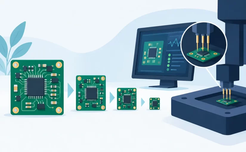
A 0201 capacitor, a 0.4 mm-pitch BGA escape route, and a densely populated RF section create the same problem from different directions: there is less physical access, less measurement margin, and more opportunity for the test method to alter the result. PCB miniaturization testing is therefore not simply conventional inspection performed with smaller probes. It is a measurement discipline built around contact geometry, parasitic effects, fixture design, test frequency, and a clear understanding of what the circuit contributes around the component under test.
PCB Miniaturization Testing Starts With Access
As component packages shrink, landing pads and exposed test points become scarce. A conventional pair of hand probes can bridge adjacent pads, scrape solder mask, or apply enough force to disturb a marginal joint. Even when contact is achieved, probe placement may add variable lead length and contact resistance that masks the value being measured.
Fine-point tweezer probes address part of this problem because they allow an operator to contact both ends of a chip resistor, capacitor, or inductor directly. The benefit is not just speed. Holding the component between closely spaced probe tips reduces the measurement loop compared with long test leads, improving repeatability on low-impedance and high-frequency measurements.
Tip selection matters. Tips that are too wide can contact solder fillets, neighboring pads, or parallel circuit paths. Tips that are excessively sharp may damage small passive components or penetrate protective coatings. For repeated production or repair work, the target is controlled contact force and repeatable placement, not maximum pressure. Operators should approach the component from a stable angle, confirm that each tip is centered on the intended termination, and release pressure as soon as a stable reading is captured.
Why Smaller Boards Produce Different Errors
Miniaturized assemblies often combine low-value passives, fast digital edges, compact power stages, and RF-sensitive traces within a small area. At that scale, the instrument, probe, and board form one measurement system.
Lead inductance and stray capacitance become more significant as component values decrease and test frequency rises. A few millimeters of probe path may be inconsequential when checking a 100 kOhm resistor at low frequency. The same geometry can materially affect measurement of a 1 nH inductor, a low-ESR ceramic capacitor, or a sub-ohm current-sense resistor. Contact resistance also becomes a dominant error source when evaluating solder joints, fuses, and low-value resistors.
This is why open and short compensation should be performed with the actual probe arrangement whenever the instrument supports it. Compensation cannot eliminate every board-level effect, but it establishes a reference for the cable, fixture, or probe tips being used. If an adapter is changed, tips are replaced, or a long lead is introduced to reach a constrained location, repeat the compensation rather than assuming the previous correction remains valid.
A stable reading is not automatically a correct reading. On a populated board, the meter may be measuring the intended component in parallel with other components, semiconductor junctions, integrated-circuit protection structures, or power rails. The correct interpretation depends on the schematic and the circuit state.
In-Circuit Measurements Need Context
An in-circuit capacitance reading can be useful for quickly comparing one location with a known-good board, identifying an obvious shorted capacitor, or screening a suspect decoupling network. It may not represent the component’s marked value. Several capacitors in parallel, nearby semiconductor paths, and residual charge can all influence the result.
Resistance measurements have similar limitations. A resistor connected to an IC input may show a value affected by internal bias networks. A low reading across a supply rail can indicate a fault, but it can also reflect normal charging behavior as the meter applies its test signal. Before assigning a failed component, compare the result with the schematic, isolate the relevant net where practical, and observe whether the measured value changes with probe polarity or test voltage.
For capacitance, inductance, and ESR work, test frequency is also part of the result. A component’s impedance behavior at 1 kHz is not the same as its behavior at 100 kHz or 250 kHz. Higher-frequency testing can reveal characteristics closer to a component’s operating environment, particularly for switching power supplies and high-speed decoupling applications. It can also make fixture and contact quality more critical. Use the frequency that answers the engineering question, rather than selecting the highest available frequency by default.
Build a Test Sequence That Protects the Board
The most efficient troubleshooting process moves from low-risk inspection to targeted electrical measurement. Start with magnification and lighting. Look for cracked terminations, tombstoned passives, solder bridges, lifted pads, discoloration, and contamination. Small defects are often easier to identify visually than electrically, especially when multiple components share the same net.
Next, verify that the board is unpowered and discharged before using resistance, LCR, or ESR functions. Large capacitors can retain charge after power removal, while sensitive IC inputs may be affected by an uncontrolled test condition. For assemblies with batteries, supercapacitors, or multiple supply domains, confirm that every energy source is disconnected.
Then establish a baseline. A known-good board, a documented production sample, or a measured reference component gives far more diagnostic value than a single isolated reading. On dense assemblies, relative comparison is often the fastest way to find an outlier. If one ceramic capacitor on a rail measures distinctly differently from identical adjacent capacitors, further investigation is justified even if the absolute in-circuit reading is not definitive.
For work instructions and quality-control procedures, define acceptance criteria before testing begins. Useful criteria include:
- permitted probe locations and the required magnification level
- instrument function, test frequency, and compensation procedure
- allowable reading range or comparison method
- whether the board must be unpowered, partially isolated, or depopulated
- required documentation for failures, rework, and retest
This level of control prevents a common failure in miniaturized-board testing: different operators reaching different conclusions because they used different contact points, frequencies, or instrument settings.
Select Instruments for the Measurement, Not the Package Size
A small handheld instrument is valuable at the bench, in field service, and on a production floor, but portability alone does not establish measurement capability. Evaluate basic accuracy, resolution, frequency range, test signal characteristics, input protection, and the physical probe system together.
For passive-component identification and board-level troubleshooting, a handheld LCR meter with direct tweezer-style contact can reduce setup time dramatically. It is particularly effective when checking unmarked SMD components, sorting removed parts, confirming resistor values, or comparing suspect passives on a board. An ESR function adds useful screening capability for capacitors in power circuits, although results must still be interpreted with the surrounding circuit in mind.
Advanced diagnostic functions can add another layer of evidence. Analog Signature Analysis compares the current-voltage response of a node or component under a controlled AC stimulus. It can help locate differences between a defective board and a reference board when a conventional resistance or capacitance reading is ambiguous. Oscilloscope capability is similarly useful when the problem is dynamic, such as an unstable supply rail, intermittent signal, or switching waveform that cannot be diagnosed with static measurements.
Siborg Systems instruments are designed around this direct-contact workflow, combining compact tweezer probing with LCR, ESR, and selected advanced measurement functions. The practical advantage is reduced handling time at the component level, provided the operator still applies the same discipline around compensation, test conditions, and circuit interpretation.
Calibration and Repeatability Are Production Requirements
Miniaturization raises the cost of a wrong decision. Removing a tiny component unnecessarily can damage pads or introduce a new assembly defect. Passing a marginal connection can create an intermittent field failure that is difficult to reproduce. Measurement confidence must therefore be supported by more than a displayed value.
Use instruments with appropriate calibration support and maintain records that connect the instrument to the work performed. A NIST-traceable calibration certificate is particularly relevant where results support quality documentation, customer returns analysis, or controlled manufacturing processes. Between formal calibrations, inspect probe tips for wear, contamination, oxidation, and loss of alignment. A damaged tip can produce inconsistent contact long before the instrument itself is out of tolerance.
Repeatability should be checked in the actual workflow. Measure a reference component or known-good board location multiple times, with normal operator handling, and observe the spread. If readings vary excessively, investigate probe pressure, tip geometry, board cleanliness, fixture movement, compensation, and test frequency before tightening acceptance limits.
Small assemblies do not make testing impossible. They make uncontrolled testing expensive. When probe access, parasitics, frequency, circuit loading, and calibration are treated as part of the measurement, compact PCBs can be evaluated quickly without sacrificing the evidence needed to make a sound repair or quality decision.